

Khi bước chân vào thế giới của cá cược, điều mà người chơi luôn quan tâm là độ tin cậy và sức hút của nhà cái đó. Danh sách 11 nhà cái uy tín hàng đầu tại Việt Nam không chỉ là một danh sách các thương hiệu nổi tiếng, mà chúng là một cuộc hành trình đầy triển vọng.
Nhà cái uy tín là những tổ chức hoặc doanh nghiệp có trách nhiệm cung cấp dịch vụ cá cược trực tuyến cho người chơi. Chúng không chỉ cung cấp một loạt các trò chơi, bao gồm thể thao, game bài đổi thưởng, casino, slot game, xổ số, bắn cá đổi thưởng, lô đề, và nhiều sự kiện giải trí khác mà còn cho phép người chơi đặt cược và thực hiện thanh toán tiền cược.

Bạn sẽ nhanh chóng phát hiện sự đa dạng trong các thương hiệu sòng bạc khác nhau trên thị trường. Tuy nhiên, khi xét đến danh sách hàng đầu về những nhà cái tốt, dưới đây là danh sách 11 thương hiệu nổi bật nhất.
M88, một trong những tên tuổi rất nổi tiếng trong lĩnh vực cá cược trực tuyến, đã gia nhập thị trường Việt Nam vào năm 2010. M88 tập trung vào việc “đặt lợi ích của người chơi cá cược lên hàng đầu” trong chiến lược hoạt động của họ. Nhà cái này đã mạnh mẽ xác lập vị thế của mình trên thị trường cá cược.

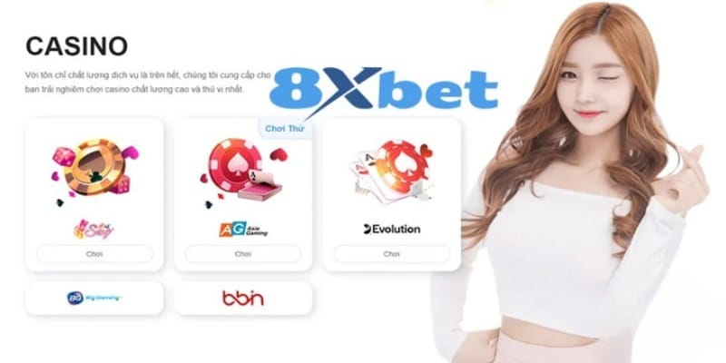
Trong suốt năm 2022 vừa qua, 8XBET đã gây ấn tượng mạnh với việc thu hút một lượng lớn người chơi tham gia. Chỉ sau một tuần từ khi ra mắt, họ đã lọt vào top 5 những nhà cái tốt nhất và chất lượng được nhiều người chơi đặt niềm tin.
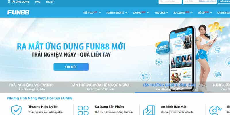
FUN88, với giao diện bắt mắt, thân thiện và ấn tượng, đã khẳng định vị thế của mình là nhà cái trực tuyến uy tín số 1 trên thị trường. Đây là một đơn vị đặt cược được đánh giá cao và cam kết mang đến một trải nghiệm chất lượng cho những người yêu thích cược.
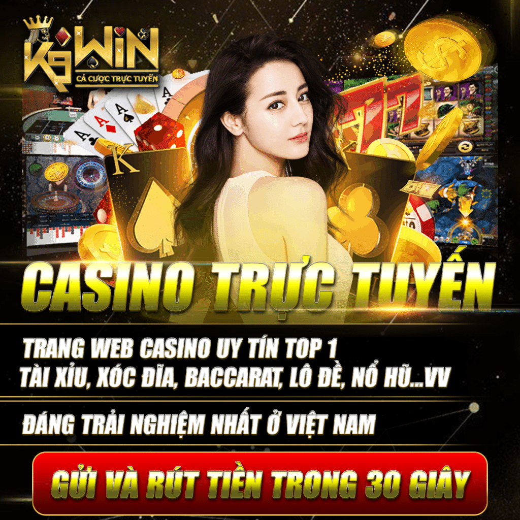
Nhà cái K9WIN đã thể hiện sự xuất sắc và được công nhận là một trong những nhà cái hàng đầu trên thị trường cá cược hiện tại. Nếu bạn đang tìm kiếm một lựa chọn đáng tin cậy để tham gia cược, thì cổng cá cược này sẽ là lựa chọn hoàn hảo cho bạn.

BK8, có trụ sở tại Malta và hoạt động dưới giấy phép cấp bởi chính phủ sở tại, đại diện cho một lựa chọn nhà cái đáng tin cậy trong lĩnh vực cá cược trực tuyến. Nhà cái này được công nhận là một địa chỉ hàng đầu trong lĩnh vực cá cược và giải trí, được đánh giá cao về tính uy tín và đã được nhiều người yêu thích.
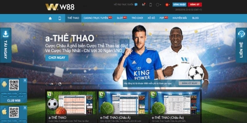
W88 ra đời vào năm 2008 và đã tích luỹ được 13 năm kinh nghiệm trong việc cung cấp dịch vụ giải trí cá cược trực tuyến. Họ được đánh giá là một nhà cái hàng đầu vì mở ra nhiều chương trình khuyến mãi hấp dẫn và giá trị tặng thưởng đáng kể cho người chơi.
Trong thị trường giải trí trực tuyến đa dạng, FB88 duy trì sự ổn định và tích cực trong các hoạt động của họ. Đặc biệt, FB88 đã được công nhận như một cái tên tiên phong trong lĩnh vực cá cược trực tuyến tại Việt Nam.

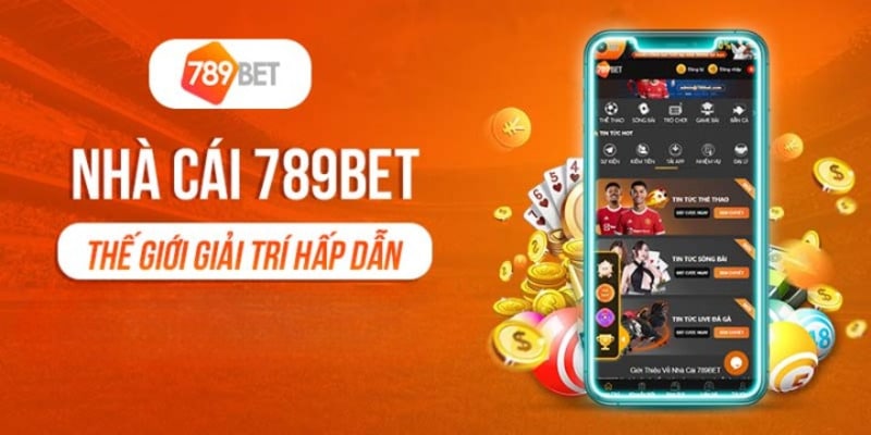
789BET, một nhà cái mới nổi tại thị trường Châu Á, đã nhanh chóng xây dựng một sự uy tín đáng kể khi so sánh với nhiều địa chỉ cá cược khác. Họ đang dần củng cố vị thế của mình trong ngành cá cược, và vì vậy, thông tin về 789BET hiện vẫn còn hạn chế và chưa được nhiều người biết đến.
NEW88 đã ghi dấu ấn với danh tiếng đáng kể trong cộng đồng người chơi tại thị trường Châu Á. Họ đã phát triển bsg mang đến một nền tảng giải trí đa dạng, được chặt chẽ giám sát bởi cơ quan quản lý trò chơi và giải trí quốc gia của Philippines.

JUN88 đứng đầu danh sách các nhà cái trực tuyến uy tín và đã thu hút sự công nhận trên thị trường cá cược thể thao, trở nên phổ biến trong cộng đồng người chơi. Nhà cái này đã nhận được giấy phép từ tổ chức kinh doanh Isle of Man, từ đó tạo thêm niềm tin đối với các thành viên tham gia.

Mặc dù Hi88 ở Việt Nam vẫn là một cái tên mới so với nhiều đối thủ khác, tuy nhiên, điều này không làm giảm sự cạnh tranh của họ với bất kỳ nhà cái nào khác. Hi88 đã nhận được giấy phép kinh doanh hợp pháp từ tổ chức cờ bạc FCRLRC, đánh dấu sự pháp lý và cam kết của nhà cái về tính minh bạch, công bằng và uy tín trong tất cả các hoạt động của họ.

Các nhà cái uy tín ở trên luôn cung cấp một trải nghiệm chất lượng với nhiều trò chơi giải trí thú vị. Bạn có thể lựa chọn một trong 11 trang web hàng đầu mà chúng tôi đã chia sẻ để tham gia vào một sân chơi an toàn, có tỷ lệ trả thưởng thuộc dạng khủng và sở hữu nhiều ưu đãi hấp dẫn.